Determining Ideal Strength and Electronic Properties of Ge/Si Core-Shell Nanowires
Copyright © The Korean Society for Precision Engineering
This is an Open-Access article distributed under the terms of the Creative Commons Attribution Non-Commercial License (http://creativecommons.org/licenses/by-nc/3.0) which permits unrestricted non-commercial use, distribution, and reproduction in any medium, provided the original work is properly cited.
Abstract
Core/shell nanowire (NW) is recognized as promising one-dimensional material for nanoelectronic and nanoelectromechanical systems. However, its mechanical properties so important for engineering applications remain largely unexplored. Based on the density functional theory (DFT), we theoretically investigate mechanical and electronic properties of the Ge-core/Si-shell NWs along the [100] direction within the cross sectional size of 1.0 nm and 1.4 nm under the axial strain. Our results show that ideal strength of Ge-core/Si-shell NWs strongly depends on wire cross sectional size compared with that of the Si and Ge NWs. Ideal strength (maximum tensile strength) of Ge-core/Si-shell NWs increases significantly when increasing thickness of the Si-shell. We found that bond lengths around interfaces between the core and the shell play a predominant role in ideal strength of Ge-core/Si-shell NWs. Additionally, band structures of NWs are modififed by applying axial strain. Band gaps of NWs decrease with increasing strain. Our results provide important insight into intrinsic mechanical behavior and electronic properties of Ge-core/Si-shell NWs, useful for the design of nanodevices with Ge-core/Si-shell NWs in future applications.
Keywords:
Ge/Si core-shell nanowires, Ideal strength, Density functional theory, Electronic properties1. Introduction
Silicon (Si) and germanium (Ge) NWs are among the most important one-dimensional (1D) semiconductors for nanoelectronic and nanoelectromechanical systems because of their availability and attractive physical properties.1-3 Their potential nanoelectronic applications involve large deformation such as flexible electronics devices and bio-nano sensors and it shows a high demand on NW elasticity, in which the elastic modulus, ideal strength and ideal strain are important parameters. For the Si NWs, the experiments showed that NWs with diameters between 15 and 60 nm can be stretched up to 7% tensile strain, with maximum fracture strengths of 12 GPa.4 The Young’s modulus of the Si NWs with a diameter less than 10 nm was measured to be 18 ± 2 GPa using an atomic force micrometer (AFM).5 For the Ge NWs, Lee et al.6 investigated that Young’s modulus of hydrogenpassivated Ge NWs depends on their crystal orientation and diameter by using ab initio calculations. Based on several empirical potentials, Kang and Cai7 has used the molecular dynamics (MD) simulation to investigate the brittle and ductile fracture of the Si and Ge NWs. Recently, the core-shell NWs by using Si and Ge have attracted considerable attention in nanodevices, due to their superior properties such as better conductance and higher mobility of charge carriage8,9 compared with that of the Si and Ge NWs. The core-shell NWs thus have potential applications in the nanoelectronic and photon devices.10-12 Experimentally, the Ge/Si NWs have been synthesized using chemical vapor deposition method successfully.13 In another experiment, the Si/Ge core-shell NWs with the <111> orientation have also fabricated.14 Theoretically, Peng et al.15 reported the effect of strain on the electronic properties of Si/Ge (Ge/Si) NWs at the level of the density functional theory (DFT). The width of the band gap in the Ge/Si NWs investigated by the DFT calculations can be tuned by the strain.16 Musin and Wang17 also studied the composition and size dependent the band gaps of the Ge/Si (Si/Ge) NWs. Liu et al.18 performed MD simulation to examine the composition-dependent Young’s modulus for the Ge/Si (Si/Ge) NWs. In addition, the thermal stress and the buckling instability in the Si/Ge (Ge/Si) NWs were investigated by Das et al..19 Although many studies have focused on synthesis, physical and electronic properties of the Si/Ge (Ge/Si) NWs,15-20 their mechanical properties have not been clarified yet. Moreover, understanding the electronic properties of Ge-core/Si-shell NWs under strain is necessary for Ge-core/Si-shell NWs design of nanostructured materials.
In this study, the DFT calculations is used to investigate the ideal strength of the Si, Ge and Ge-core/Si-shell NWs with the cross sectional sizes of 1.0 and 1.4 nm under uniaxial tension. The ideal strength of the NWs increase with increasing of the wire cross sectional size, in which the ideal strength of Ge-core/Si-shell NWs increases significantly compared with that of the Si and Ge NWs. Furthermore, the effects of strain on the energy band structure of Ge-core/Si-shell NWs has also been discussed as well.
2. Methodology
First-principles DFT calculations are used to investigate the mechanical and electronic properties of the Si, Ge and Ge-core/Si-shell NWs. Quantum-ESPRESSO (QE) package21 is used for the firstprinciple calculations, which is a full DFT simulation package using a plane-wave basic set with pseudopotentials. The ultrasoft pseudopotentials22 with the cutoff energy of plane wave of 45 Ry is used, and the exchange-correlation energy is evaluated by the general-gradient approximation using the Perdew-Burke-Ernzerhof23 function.
The atomic structures of the Si, Ge and Ge/Si core-shell NWs for DFT are shown in Fig. 1, in which the Si and Ge atoms are initially positioned at their bulk lattice sites with the lattice constants of 5.42 A and 5.63 A respectively and the surfaces of wires are passivated by hydrogen. The cross sectional size, D, in unit of nanometer is defined as the distance between two outer shell atoms. The cross sectional size of Ge core is 0.4 nm. All systems are set by a vacuum space of 12 A in the direction perpendicular to the wire axis to avoid virtual interactions from the neighboring nanowires under the periodic boundary condition. The k-point grids in the Brillouin-zone selected according to the Monkhorst-Pack method24 is 1 × 1 × 8 and 1 × 1 × 6 for the cross sectional size D of 1.0 and 1.4 nm, respectively.
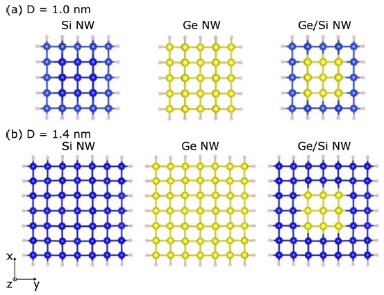
(Color online) Snapshots of the Si, Ge, and Ge/Si core-shell NWs are viewed from the cross section. The core atoms are Ge, the shell atoms are Si, and pink balls on the surface are H atoms. The cross sectional sizes of wires are (a) 1.0 and (b) 1.4 nm, respectively. The cross sectional size of Ge core is 0.4 nm. Blue, yellow, and pink balls represent the Si, Ge, and H atoms, respectively
To simulate the effect of tensile strain in the Si, Ge and Ge/Si NWs, first, the atomic positions and the cell dimensions in the z direction of all models are relaxed by using the Broyden Fretcher-Goldfarb-Shanno (BFGS) minimization method until all the Hellmann–Feynman forces and the normal component of the stress are less than 0.0005 Ry/a.u. and 0.05 GPa, respectively. Then, the loading strain is applied to the models by elongating the cell along the z direction with an increment of 0.02. The strain is refined with a very small increment of 0.005 at locations near the fracture point, and the atomic structure is fully relaxed under fixed cell dimensions after each increment of the strain. Here, the tensile strain is defined as εzz = ΔL/L0, where L0 is the length of the unit cell at geometry optimization and ΔL is the increment of the length under tension. In the energy band structure calculations, the number of k-points are scanned along the reciprocal direction from Γ to X of 50.
3. Results and Discussion
Table 1 lists the diameters D0 and the lengths L0 of the relaxed structure of the Si, Ge and Ge-core/Si-shell NWs, in which the structures are locally stables at the local minimum of the total energy. The most basic mechanical property of the NWs is the Young’s modulus, E, which is defined as follows.25

Equilibrium configurations including number of atom in unit cell N, length D0, diameter L0, Young’s modulus E, Poisson’s ratio ν, ideal strains εzz, and ideal strength σzz for different Si, Ge, and Ge-core/Si-shell NWs
| (1) |
where U is the strain energy, V0 is the equilibrium volume and εzz is the uniaxial strain. The small strains (± 0.005; ± 0.01; ± 0.015; ± 0.02) was applied, which stay in the harmonic regime. The total energy and the atomic positions as a function of the axial strain imposed on the nanowire are obtained, since the Young’s modulus can be calculated by fitting a second degree polynomial to U(ε). E of the Si, Ge and Ge-core/Si-shell NWs are listed in Table 1. These results agree reasonably well with the previously reported DFT results for Si NWs,26 Ge NWs6 and Ge-core/Si-shell NWs.15 E of all Si, Ge and Ge/Si NWs increases with increasing the wire cross sectional size D. Moreover, E of Ge-core/Si-shell NWs is smaller than that of Si NWs, but it is higher than that of Ge NWs with the same wire sizes, which is attributed to the Si component in the Ge-core/Si-shell NWs. It is well-know that E in bulk Ge is smaller than that in bulk Si,15 thus the Young’s modulus of Si NWs investigated is higher than that of Ge and Ge-core/Si-shell NWs at the same wire cross sectional size.
In Fig. 2, we show the stress-strain curves of the Si, Ge, and Ge-core/Si-shell NWs under the tensile strain. The stress computed from QE package21 is automatically evaluated over the entire supercell volume Vcell. Therefore, the supercell stress by Vcell/V0 is rescaled to obtain the stress of the nanowires.25,27 The obtained results show that the ideal strength of the Si, Ge and Ge-core/Si-shell NWs increases with increasing the wire cross sectional size. In particular, the ideal strength of Ge-core/Si-shell NWs strongly depends on the wire cross sectional size compared with the ideal strength of Si and Ge NWs. The ideal strength of Ge/Si NWs increases by 28% comparing with 7.23% and 2.5% of Si and Ge NWs, respectively. In order to understand these behavious, the detailed deformation and failure mechanisms of the structures and bonds of the NWs are investigated, as shown in Fig. 3. The atomic positions and the typical bond lengths under different tensile strains are extracted to reveal the tensile deformation mechanism of the Si, Ge, and Ge-core/Si-shell NWs.
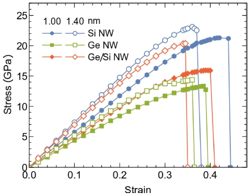
(Color online) Tensile stress along axial direction of different NWs plotted as a function of strain
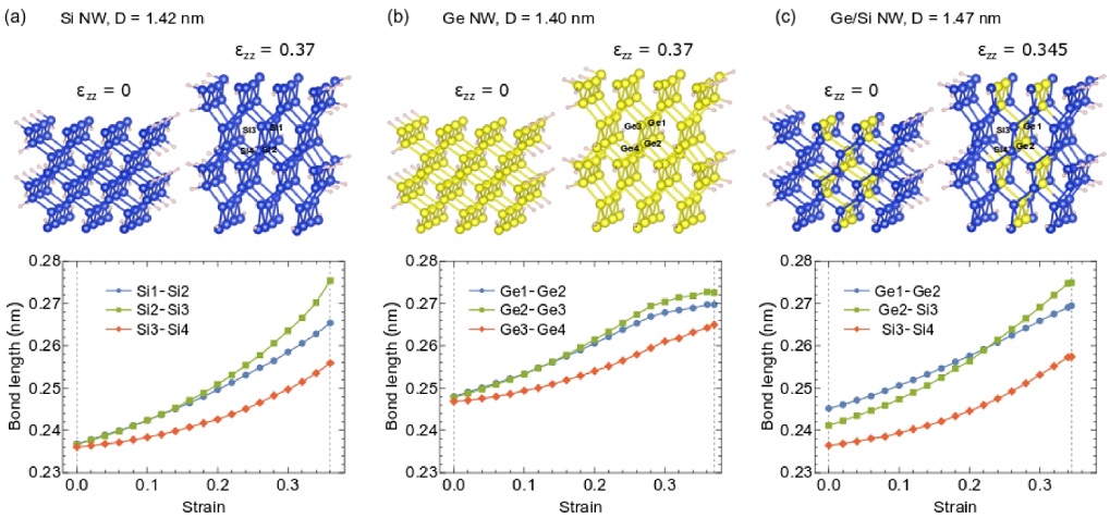
(Color online) Perspective view of the atomic structures at unstrain (εzz = 0) and ideal strains (εzz = 0.37 for Si and Ge NWs, and εzz = 0.345 for Ge-core/Si-shell NWs) with the bond lengths: (a) (Si1-Si2, Si2-Si3, Si3-Si4) in Si NW, (b) (Ge1-Ge2, Ge2-Ge3, Ge3-Ge4) in Ge NW, and (c) (Ge1-Ge2, Ge2-Si3, Si3-Si4) in Ge-core/Si-shell NW. Blue, yellow, and pink balls represent the Si, Ge, and H atoms, respectively
In Fig. 3, we show the atomic positions of 1.4 nm Si, Ge and Ge/Si NWs at the unstrain (ε = 0) and the ideal strains (ε = 0.37 for the Si and Ge NWs, and ε = 0.345 for Ge/Si NWs cases). In the unstrain case (ε = 0), the bond lengths in the Si NW (Si1-Si2, Si2-Si3 and Si3-Si4) and the Ge NW (Ge1-Ge2, Ge2-Ge3 and Ge3-Ge4) are approximated by 0.2360 nm and 0.247 nm, respectively. On the other hand, the bond lengths of the Ge-core/Si-shell NWs (Ge1-Ge2, Ge2-Si3 and Si3-Si4) are different around the interface between the Ge-core and the Si-shell. The results show that the Ge1-Ge2 bond length of the Ge-core/Si-shell NW (0.245 nm) is smaller than that of the Ge NW (0.247 nm), while the Si3-Si4 bond length of Ge-core/Si-shell NW (0.2364 nm) is higher than that of the Si NW (0.2360 nm). This could be explained that the interface atoms of Ge-core in the Ge-core/Si-shell NW are compressively strained by the Si-shell, meanwhile the Si-shell atoms are tensibly strained by the Ge-core. Therefore, the Ge2-Si3 bond length (0.241 nm) is smaller than that of Si3-Si4 bond length and higher than that of Ge1-Ge2 bond length. The bond lengths in the Si, Ge and Ge-core/Si-shell NWs increase as a function of tensile strain. The Ge1-Ge2 bond length in the Ge-core/Si-shell NW increases of 9.9% compared with 8.76% of the Ge1-Ge2 in the Ge NW. In addition, the Si3-Si4 bond length in the Ge-core/Si-shell NW increases of 8.86% compared with 8.4% of the Si3-Si4 in the Si NW. The different deformation of the bond lengths around the interface between the Ge-core and Si-shell will contribute to the mechanical properties of the Ge-core/Si-shell NWs. Furthermore, by decreasing the wire cross sectional size, the atoms around the interface will contribute significantly to the mechanical properties of the core-shell NWs, which leads to the ideal strength of the Ge-core/Si-shell NWs strongly depends on the wire cross sectional size compared with that of the Si and Ge NWs.
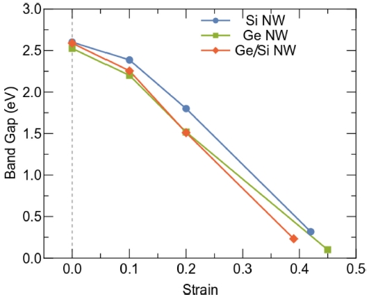
To understand the electronic properties of NWs under strain, we calculate the energy band structures of the Si, Ge and Ge/Si NWs with diameter of 1.0 nm at the different uniaxial strain. It is well-known that the band gap of the NWs is defined by the energy different between the conduction band edge (CBE) and the valance band edge (VBE).15 As shown in the Figs. 4(a)-4(c), the electronic structures of the Si, Ge and Ge-core/Si-shell NWs are calculated at the unstrain (εzz = 0), strain (εzz = 0.2) and ideal strain (εzz = 0.42, 0.405 and 0.39) for the Si, Ge and Ge-core/Si-shell NWs, respectively. It can be seen that the band structure of the NWs are significantly modulated by strain, which is in good agreement with previous studies.15 At the unstrain (εzz = 0), the Si and Ge/Si NWs are direct-gap semiconductors with the band gap of 2.60 eV and 2.59 eV, respectively, while Ge NW is indirect-gap semiconductor with band gap of 2.53 eV. It is interesting to note that the band gap of the Ge-core/Si-shell NW is smaller than that of the Si NW, while it is higher than that of Ge NW at the same wire sizes because of the composition effect in the Ge-core/Si-shell NW. When the strain is applied and gradually increases, the band structure of the NWs is substantially modified. At the strain of εzz = 0.2, Si, Ge and Ge-core/Si-shell NWs are indirect-gap semiconductor with band gap of 1.8 eV, 1.52 eV and 1.51 eV, respectively. At the ideal strain, Si, Ge and Ge-core/Si-shell NWs are direct-gap semiconductor with band gap of 0.32 eV, 0.10 eV and 0.23 eV, respectively. These results suggest that not only band gap but also direct-/indirect-gaps of the NWs can be controlled by applying strain. As shown in Fig. 5, the band gaps of Si, Ge and Ge-core/Si-shell NWs with the diameter of 1.0 nm are plotted as a function of the strain, in which the band gaps of the NWs decrease with increasing strain. This trend is also observed in previous studies for the Si28and Ge6,29, and Ge-core/Si-shell NWs.15,16
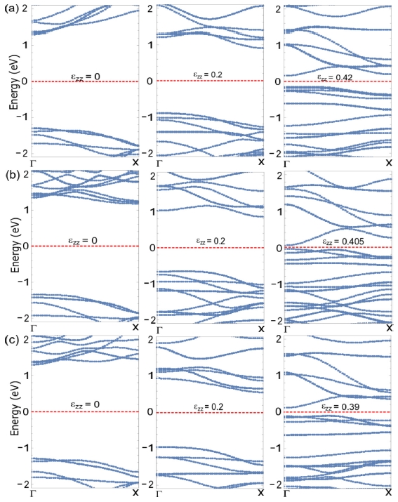
(Color online) Energy band structure of the (a) Si NW, (b) Ge NW, and (c) Ge-core/Si-shell NW with diameter of 1.0 nm in the [100] direction at the different uniaxial strain
4. Conclusion
In summary, the ideal strength and the energy band structure of the Si, Ge and Ge-core/Si-shell NWs under tensile strain are evaluated by using the first-principles DFT calculations. The results obtained show that the ideal strength of the Ge-core/Si-shell NWs strongly depends on the wire cross sectional size compared with that of the Si and Ge NWs. This phenomenon originates from the different of bond lengths around the interfaces between the Ge-core and Si-shell. Furthermore, the band structure of NWs can be modulated by using the external uniaxial strain. The band gap of the NWs decreases with increasing strain. Based on the results of this study, it is possible to better understand the mechanical and electronic properties of the Ge-core/Si-shellNWs, which are useful for the design and fabrication of nanoelectromechanical devices with the Ge-core/Si-shell NWs.
Acknowledgments
This paper was presented at PRESM 2019
This work was supported by the Vietnam’s National Foundation for Science and Technology Development (NAFOSTED) with No. 107.02-2016.18.
REFERENCES
-
Xia, Y., Yang, P., Sun, Y., Wu, Y., Mayers, B., et al., “One Dimensional Nanostructures: Synthesis, Characterization, and Applications,” Advanced Materials, Vol. 15, No. 5, pp. 353-389, 2003.
[https://doi.org/10.1002/adma.200390087]

-
Yan, R., Gargas, D., and Yang, P., “Nanowire Photonics,” Nature Photonics, Vol. 3, No. 10, pp. 569-576, 2009.
[https://doi.org/10.1038/nphoton.2009.184]

-
Wan, Y., Sha, J., Chen, B., Fang, Y., Wang, Z., et al., “Nanodevices based on Silicon Nanowires,” Recent Patents on Nanotechnology, Vol. 3, No. 1, pp. 1-9, 2009.
[https://doi.org/10.2174/187221009787003348]

-
Zhu, Y., Xu, F., Qin, Q., Fung, W. Y., and Lu, W., “Mechanical Properties of Vapor-Liquid-Solid Synthesized Silicon Nanowires,” Nano Letters, Vol. 9, No. 11, pp. 3934-3939, 2009.
[https://doi.org/10.1021/nl902132w]

-
Kizuka, T., Takatani, Y., Asaka, K., and Yoshizaki, R., “Measurements of the Atomistic Mechanics of Single Crystalline Silicon Wires of Nanometer Width,” Physical Review B, Vol. 72, No. 3, Paper No. 035333, 2005.
[https://doi.org/10.1103/PhysRevB.72.035333]

-
Lee, A. J., Kim, M., Lena, C., and Chelikowsky, J. R., “Mechanical and Electronic Properties of Strained Ge Nanowires Using ab Initio Real-Space Pseudopotentials,” Physical Review B, Vol. 86, No. 11, Paper No. 115331, 2012.
[https://doi.org/10.1103/PhysRevB.86.115331]

-
Kang, K. and Cai, W., “Brittle and Ductile Fracture of Semiconductor Nanowires–Molecular Dynamics Simulations,” Philosophical Magazine, Vol. 87, Nos. 14-15, pp. 2169-2189, 2007.
[https://doi.org/10.1080/14786430701222739]

-
Xiang, J., Lu, W., Hu, Y., Wu, Y., Yan, H., et al., “Ge/Si Nanowire Heterostructures as High-Performance Field-Effect Transistors,” Nature, Vol. 441, No. 7092, pp. 489-493, 2006.
[https://doi.org/10.1038/nature04796]

-
Goldthorpe, I. A., Marshall, A. F., and McIntyre, P. C., “Synthesis and Strain Relaxation of Ge-Core/Si-Shell Nanowire Arrays,” Nano Letters, Vol. 8, No. 11, pp. 4081-4086, 2008.
[https://doi.org/10.1021/nl802408y]

-
Goldthorpe, I. A., Marshall, A. F., and McIntyre, P. C., “Inhibiting Strain-Induced Surface Roughening: Dislocation-Free Ge/Si and Ge/Sige Core-Shell Nanowires,” Nano Letters, Vol. 9, No. 11, pp. 3715-3719, 2009.
[https://doi.org/10.1021/nl9018148]

-
Zhao, Y., Smith, J. T., Appenzeller, J., and Yang, C., “Transport Modulation in Ge/Si Core/Shell Nanowires through Controlled Synthesis of Doped Si Shells,” Nano Letters, Vol. 11, No. 4, pp. 1406-1411, 2011.
[https://doi.org/10.1021/nl1031138]

-
Fukata, N., Mitome, M., Sekiguchi, T., Bando, Y., Kirkham, M., et al., “Characterization of Impurity Doping and Stress in Si/Ge and Ge/Si Core–Shell Nanowires,” ACS Nano, Vol. 6, No. 10, pp. 8887-8895, 2012.
[https://doi.org/10.1021/nn302881w]

-
Lauhon, L. J., Gudiksen, M. S., Wang, D., and Lieber, C. M., “Epitaxial Core–Shell and Core–Multishell Nanowire Heterostructures,” Nature, Vol. 420, No. 6911, pp. 57-61, 2002.
[https://doi.org/10.1038/nature01141]

-
Morales, A. M. and Lieber, C. M., “A Laser Ablation Method for the Synthesis of Crystalline Semiconductor Nanowires,” Science, Vol. 279, No. 5348, pp. 208-211, 1998.
[https://doi.org/10.1126/science.279.5348.208]

-
Peng, X., Tang, F., and Logan, P., “First Principles Study of Si/Ge Core-Shell Nanowires--Structural and Electronic Properties,” In: Nanowires-Fundamental Research, Hashim, A. A., (Ed.), InTech, Chap. 4, 2011.
[https://doi.org/10.5772/16298]

-
Liu, N., Lu, N., Yao, Y.-X., Li, Y.-R., Wang, C.-Z., et al., “Strain Effects in Ge/Si and Si/Ge Core/Shell Nanowires,” The Journal of Physical Chemistry C, Vol. 115, No. 32, pp. 15739-15742, 2011.
[https://doi.org/10.1021/jp110379n]

-
Musin, R. N. and Wang, X.-Q., “Quantum Size Effect in Core-Shell Structured Silicon-Germanium Nanowires,” Physical Review B, Vol. 74, No. 16, Paper No. 165308, 2006.
[https://doi.org/10.1103/PhysRevB.74.165308]

-
Liu, X. W., Hu, J., and Pan, B. C., “The Composition-Dependent Mechanical Properties of Ge/Si Core–Shell Nanowires,” Physica E: Low-Dimensional Systems and Nanostructures, Vol. 40, No. 10, pp. 3042-3048, 2008.
[https://doi.org/10.1016/j.physe.2008.03.011]

-
Das, S., Moitra, A., Bhattacharya, M., and Dutta, A., “Simulation of Thermal Stress and Buckling Instability in Si/Ge and Ge/Si Core/Shell Nanowires,” Beilstein Journal of Nanotechnology, Vol. 6, No. 1, pp. 1970-1977, 2015.
[https://doi.org/10.3762/bjnano.6.201]

-
Varahramyan, K. M., Ferrer, D., Tutuc, E., and Banerjee, S. K., “Band Engineered Epitaxial Ge–Six Ge1–x Core-Shell Nanowire Heterostructures,” Applied Physics Letters, Vol. 95, No. 3, Paper No. 033101, 2009.
[https://doi.org/10.1063/1.3173811]

-
Giannozzi, P., Baroni, S., Bonini, N., Calandra, M., Car, R., et al., “Quantum Espresso: A Modular and Open-Source Software Project for Quantum Simulations of Materials,” Journal of Physics: Condensed Matter, Vol. 21, No. 39, Paper No. 395502, 2009.
[https://doi.org/10.1088/0953-8984/21/39/395502]

-
Rappe, A. M., Rabe, K. M., Kaxiras, E., and Joannopoulos, J. D., “Optimized Pseudopotentials,” Physical Review B, Vol. 41, No. 2, pp. 1227-1230, 1990.
[https://doi.org/10.1103/PhysRevB.41.1227]

-
Perdew, J. P., Burke, K., and Ernzerhof, M., “Perdew, Burke, and Ernzerhof Reply,” Physical Review Letter, Vol. 80, No. 4, pp. 891, 1998.
[https://doi.org/10.1103/PhysRevLett.80.891]

-
Monkhorst, H. J. and Pack, J. D., “Special Points for Brillouin-Zone Integrations,” Physical Review B, Vol. 13, No. 12, pp. 5188-5192, 1976.
[https://doi.org/10.1103/PhysRevB.13.5188]

-
Hung, N. T., Van, T. V., and Saito, R., “Intrinsic Strength and Failure Behaviors of Ultra-Small Single-Walled Carbon Nanotubes,” Computational Materials Science, Vol. 114, pp. 167-171, 2016.
[https://doi.org/10.1016/j.commatsci.2015.12.036]

-
Lee, B. and Rudd, R. E., “First-Principles Study of the Young’s Modulus of Si<001> Nanowires,” Physical Review B, Vol. 75, No. 4, Paper No. 041305, 2007.
[https://doi.org/10.1103/PhysRevB.75.041305]

-
Hung, N. T. and Truong, D. V., “Ab initio Study of Structural Transition and Pseudoelasticity in Cu Nanowires,” Surface Science, Vol. 641, pp. 1-5, 2015.
[https://doi.org/10.1016/j.susc.2015.05.004]

-
Leu, P. W., Svizhenko, A., and Cho, K., “Ab initio Calculations of the Mechanical and Electronic Properties of Strained Si Nanowires,” Physical Review B, Vol. 77, No. 23, Paper No. 235305, 2008.
[https://doi.org/10.1103/PhysRevB.77.235305]

-
Logan, P. and Peng, X., “Strain-Modulated Electronic Properties of Ge Nanowires: A First-Principles Study,” Physical Review B, Vol. 80, No. 11, Paper No. 115322, 2009.
[https://doi.org/10.1103/PhysRevB.80.115322]


Lecturer-Ph.D in the School of Mechanical Engineering, Hanoi University of Science and Technology, Hanoi, Vietnam. His research interest are fracture mechanics, artificial muscles and nanomechanics.
E-mail: thanh.vuongvan@hust.edu.vn

Assistant Professor in Frontier Research Institute for Interdisciplinary Sciences, Tohoku University, Sendai 980-8578, Japan. His research interest are thermoelectricity, artificial muscles and nanomechanics.
E-mail: nguyen@flex.phys.tohoku.ac.jp

Ph.D. student in the School of Mechanical Engineering, Hanoi University of Science and Technology, Hanoi, Vietnam. His research interest is studying on fracture mechanics at the scales of atom, nanometer and micro meter.
E-mail: tranthequang12@gmail.com

Lecturer -Assoc. Professor in the School of Mechanical Engineering, Hanoi University of Science and Technology, Hanoi, Vietnam. His research interest is studying on fracture mechanics at the scales of atom, nanometer and micro meter (simulation and experiment).
E-mail: truong.dovan@hust.edu.vn

