Micro Hole Machining Characteristics of Glassy Carbon Using Electrical Discharge Machining (EDM)
Copyright © The Korean Society for Precision Engineering
This is an Open-Access article distributed under the terms of the Creative Commons Attribution Non-Commercial License (http://creativecommons.org/licenses/by-nc/3.0) which permits unrestricted non-commercial use, distribution, and reproduction in any medium, provided the original work is properly cited.
Abstract
Glassy carbon (GC) has superior properties such as high corrosion resistance, heat resistance, and low adhesion to glass materials in a glass molding process (GMP). In addition, the demand for GC molds is increasing in various industries that require high precision of glass parts. However, GC is a difficult-to-machine material with high hardness and brittleness. Electrical discharge machining (EDM) can machine GC regardless of its strength or hardness. In this study, tungsten carbide (WC-Co) electrode was fabricated by wire electrical discharge grinding (WEDG). Characteristics of EDM of micro holes on GC were then analyzed. As capacitance and voltage increased, material removal rate (MRR) increased while machining time tended to decrease. However, at low voltages, short circuit and secondary discharge occurred, which increased the electrode wear rate (EWR). As a result, a D-shaped electrode that could prevent short circuit and debris accumulation was fabricated and a micro hole array was machined.
Keywords:
EDM, Glassy carbon, Micro hole, Material removal rate, Electrode wear, Secondary discharge키워드:
방전 가공, 유리질 탄소, 미세 구멍, 재료 제거율, 전극 마모, 이차 방전1. Introduction
In microsystems technology, glass-based components with welldefined shapes and strict tolerances are required, and various studies have been conducted on fabricating glass-based components [1]. The geometries required in glass microstructures include microchannels, microgrooves, microlens arrays and micropillar arrays [2]. Glass molding process (GMP) is a suitable method for mass producing glass-based components at low cost and high productivity [3]. Among the various mold materials, glassy carbon (GC) is widely used as a mold material due to its superior heat resistance, corrosion resistance, low adhesion to glass materials, and minimal damage during the cooling process [4]. However, GC is a difficult-to-machine material with high hardness, and brittle fracture such as cracks and edge chipping can occur in the machined area during mechanical machining processes [5]. Therefore, various non-conventional machining processes for fabricating GC have been studied. Haq et al. [4] fabricated GC molds with a high-quality microstructure through the carbonization of a replicated furan precursor. Tseng et al. [6] fabricated GC molds using an ultraviolet laser processing system, which were subsequently used to form microchannel chips with soda-lime glass. Youn et al. [7] conducted repetitive-pass milling with a focused ion beam (FIB) for maskless and resistless fabrication of GC molds.
Electrical discharge machining (EDM) is a non-conventional machining process that removes material by converting electrical energy into thermal energy through a series of successive sparks generated between the electrode and the workpiece in a dielectric fluid [8-12]. Furthermore, EDM does not require direct contact between the electrode and the workpiece eliminating mechanical stresses, chatter and vibration problems during machining [13]. Muramatsu et al. [14] performed EDM on glassy carbon, exploring machining conditions according to working fluid, electrode rotational speed, voltage and duty factor. However, previous studies have primarily focused on the fabricating molds and dies for forming optical glass devices, and there is a lack of research on the machining of micro holes on GC.
Therefore, this study used EDM to fabricate micro holes on GC and investigated the influence of EDM parameters on the material removal rate (MRR), electrode wear ratio (EWR), surface roughness.
2. Experimental Setup
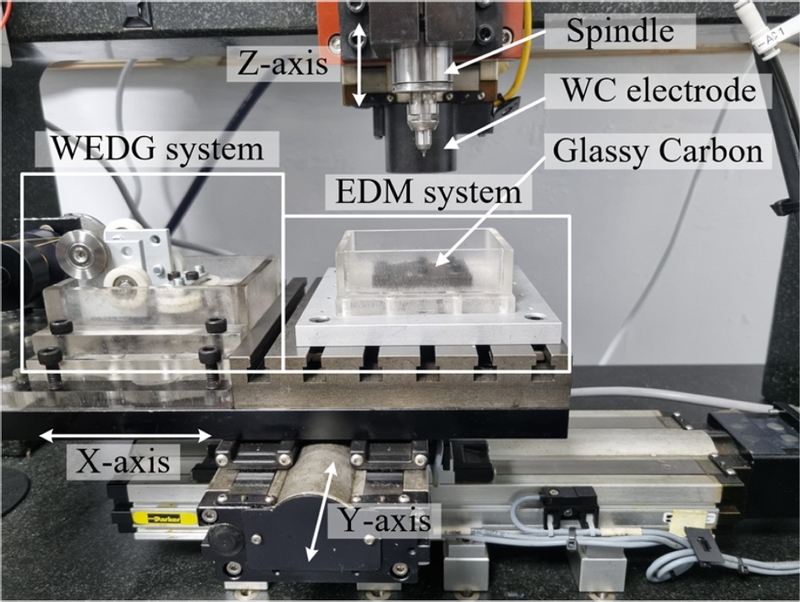
Fig. 1 shows the experimental setup of the machining system. The machining system consists of a 3-axis precision stage and a spindle, a WEDG system for electrode fabrication, an RC discharge circuit, and an EDM system including a discharge tank. The WEDG system and EDM system are integrated into an in-situ system to prevent potential errors and runout during electrode mounting [15]. The GC substrate was mounted on the EDM system. Material properties of GC used in this study are shown in Table 2.
The RC discharge circuit consists of a power supply, a resistor and a capacitor. Discharge current was collected through the AD board and used as a feedback signal to prevent short circuits. Furthermore, the composition variation of the machined area was analyzed using confocal Raman microscopy (inViaTM InSpect Confocal Raman Microscope, Renishaw Corp.), while the geometry of the machined micro holes and electrode wear were analyzed using a confocal microscope (OLS-5000, Olympus Corp.) and a scanning electron microscope (FE-SEM, Carl Zeiss Corp.).
3. Experimental Method
3.1 Fabrication of WC-Co Electrode
Through the WEDG system, micro tools or electrodes can be fabricated into various geometries [17,18]. WC-Co was used as the electrode material. Tungsten carbide (WC-Co) possesses a high melting temperature, good thermal conductivity, and high mechanical rigidity, which makes it a suitable material for micro electrodes for EDM [19]. The electrode fabrication process is as follows: A brass wire connected to the cathode is transported at a constant speed along a guide. An WC-Co rod with a diameter of 1 mm is connected to the anode and rotated at 1000 rpm. The rotating electrode is transported vertically along the Z-axis. Electrical discharge occurs in the gap between the brass wire and the WC-Co rod, fabricating the cylindrical electrode. Debris flushing occurs simultaneously with electrode fabrication due to the rotation of the rod.
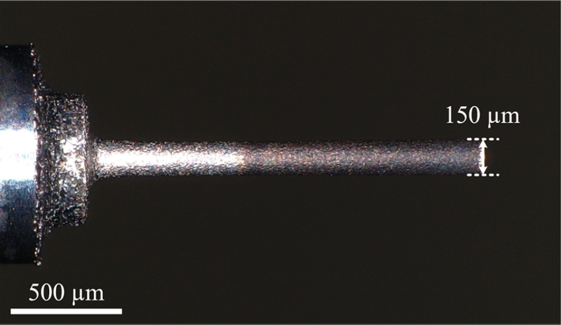
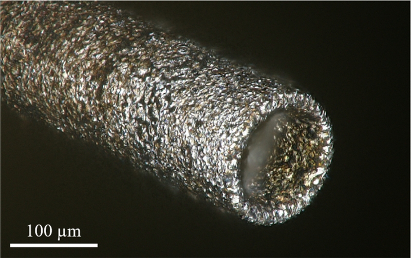
The electrode fabrication conditions are shown in Table 1. Fig. 2 shows the optical image of a cylindrical WC-Co electrode fabricated via WEDG with a diameter of 150 μm.
3.2 EDM of GC
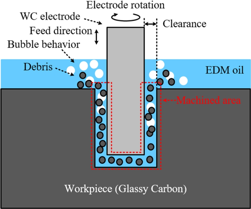
Fig. 3 is a schematic diagram of the micro hole machining process. The electrode is rotated at a constant speed of 3,000 rpm and micro holes are machined on GC substrates by transporting the electrode at a feed rate of 5 μm/s. The discharge current is collected through the AD board in real time and used as a feedback signal during micro holes machining. If a short circuit occurs due to contact between the electrode and GC, the electrode is raised by 10 μm to maintain the gap. Additionally, dielectric fluid exchange and debris flushing are performed through bubble behavior that occurs during EDM [20]. Kerosene was used as the dielectric fluid to cool the machined area and restore insulation between GC and electrode.
EDM using an RC discharge circuit, the discharge energy (E) depends on the capacitance (C) and the voltage (V), as shown in Eq. (1). Increasing the voltage and capacitance causes discharge energy to rise, resulting in large discharge craters on the surface of the workpiece [15].
| (1) |
To analyze the machining characteristics according to the capacitance, micro holes with a depth of 600 μm were machined using various capacitances with an applied voltage of 100 V. Additionally, micro holes with a depth of 600 μm were machined using various voltages with a capacitance of 5,000 pF to analyze the machining characteristics according to voltage. Micro hole machining conditions are shown in Table 3. During micro hole machining, MRR, EWR, and other machining conditions were analyzed based on measured machining time, clearance, tool wear length. MRR is the amount of material removed per unit time and is calculated by the diameter (D) and depth (t) of the micro hole and the machining time (T) as shown in Eq. (2). EWR is approximated by the ratio of the tool wear length (Le) and machining depth as shown in Eq. (3) [21].
| (2) |
| (3) |
4. Experimental Results and Discussion
4.1 Effects of Capacitance
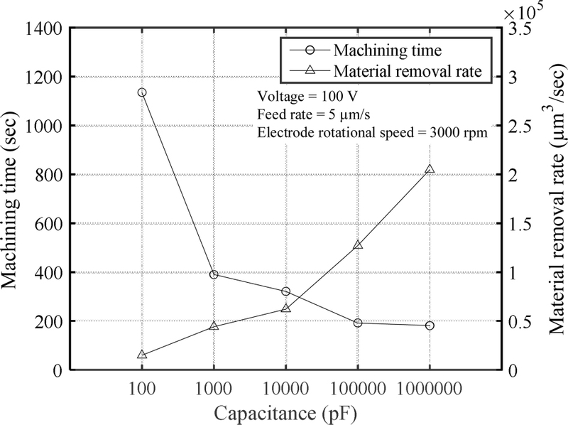
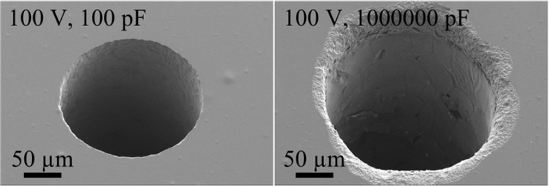
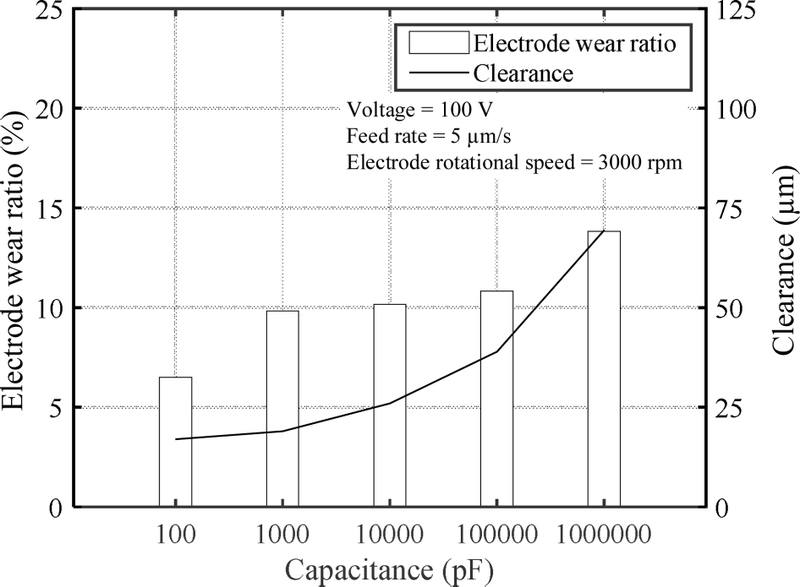
The machining characteristics according to capacitance were analyzed at an applied voltage of 100 V, feed rate of 5 μm/s, and rotational speed of 3,000 rpm. Fig. 4 shows the machining time and MRR according to capacitance. As the capacitance increased, the MRR increased and the machining time decreased. This was caused by the increased single discharge energy with higher capacitance. However, as shown in Figs. 5 and 6, when using a capacitance of 1,000,000 pF, the high discharge energy caused the melting of GC, resulting in a relatively large clearance. Additionally, as the capacitance increased, both the EWR and clearance increased. This was due to the high discharge energy, which led to GC removal and electrode wear concurrently.
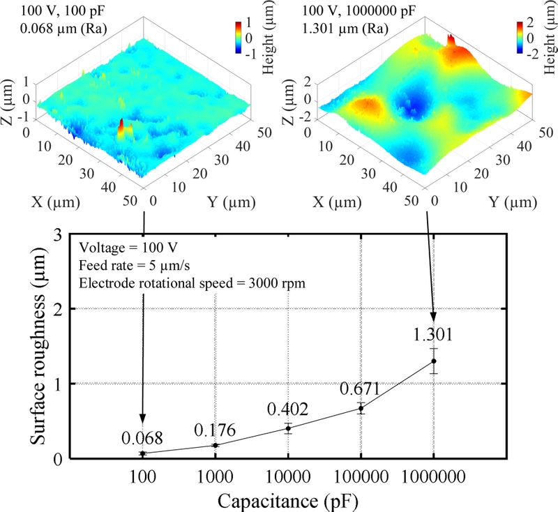
Fig. 7 shows surface roughness according to capacitance and the E 3D profiles of machined area. As the capacitance increased, the single discharge energy increased, resulting in the overlapping of relatively large discharge craters, which led to an increase in the average surface roughness (Ra).
4.2 Effects of Voltage
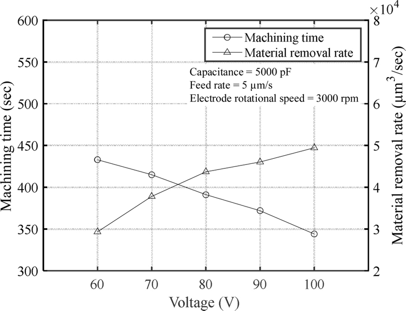
Under a capacitance of 5,000 pF, a feed rate of 5 μm/s, and a rotational speed of 3,000 rpm, the machining characteristics according to voltage were analyzed. Fig. 8 shows the machining time and MRR according to voltage. As the voltage increased, the MRR increased due to the rise in single discharge energy, and the machining time decreased accordingly.
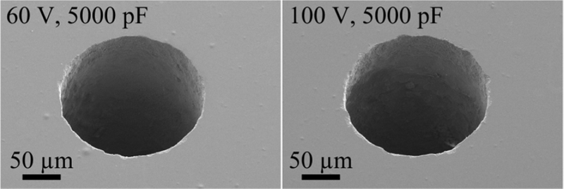
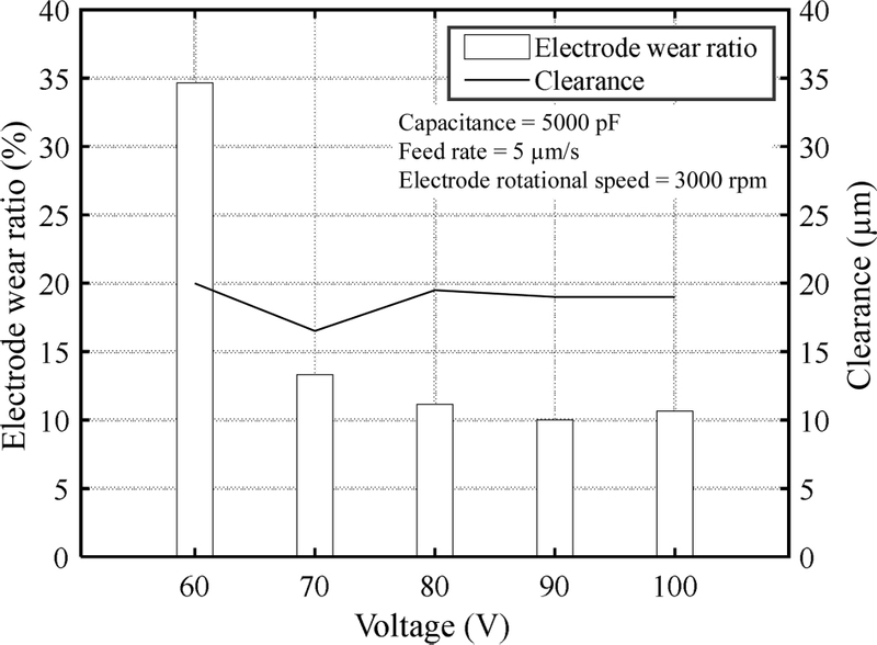
Fig. 9 shows the machined hole shape according to voltage. Applying a voltage of 100 V resulted in a slightly smaller geometric error of the micro hole compared to an applied voltage of 60 V. However, as shown in Fig. 10, the EWR tended to increase as the applied voltage decreased, with the highest EWR observed at applied voltage of 60 V. Additionally, the clearance did not change significantly. This indicates that the single discharge energy was relatively small in this machining condition, which led to frequent short circuits and increased EWR. Generated debris also induced secondary discharges as it was flushed out through the clearance. Despite the reduction in single discharge energy, the clearance remained largely unchanged [22,23]. Secondary discharge refers to uneven electrical discharges caused by generated debris, which leads to a reduction in the geometric accuracy of the machined area [24,25].
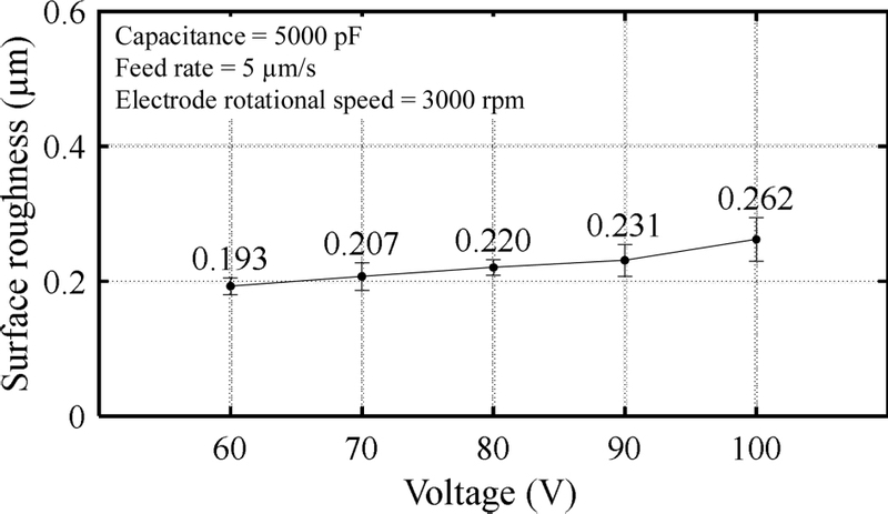
Fig. 11 shows the surface roughness according to voltage. Since the applied voltage increased in increments of 10 V, the corresponding increase in discharge energy was relatively small, resulting in only a slight increase in surface roughness.
4.3 Electrode Wear
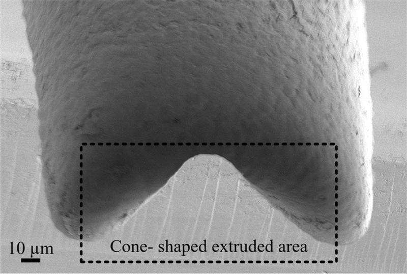
Fig. 12 shows the electrode wear after machining 20 micro holes at an applied voltage of 60 V and a capacitance of 5,000 pF. The center of the electrode was worn into a concave-shaped with a measured depth of 134 μm. Since the rotational speed at the electrode center converged to zero, the generated debris accumulated and remained suspended between the electrode center and the bottom of the micro holes. Consequently, electrical discharge occurred between the electrode center and the suspended debris, leading to wear of the concave-shaped electrode [26-28]. Continuous machining with a concave-shaped electrode resulted in the bottom of the micro hole being extruded into a cone shape, as shown in Fig. 13. Furthermore, debris flushing became inefficient as the machined hole depth increased, leading to short circuits. During this process, secondary discharges occurred between the electrode and the hole wall, causing uneven electrode wear.
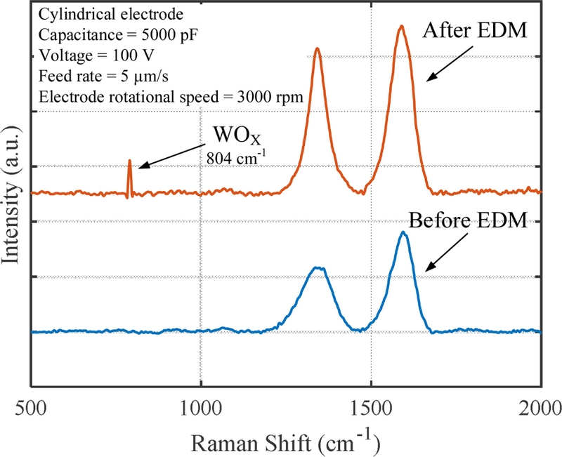
Fig. 14 shows the Raman spectrum of the machined area. A peak value of 804 cm-1 appeared, representing tungsten oxide (WOX), indicating that the electrode melted and adhered to the GC during EDM [29,30].
4.4 Improving Machinability with Debris Flushing
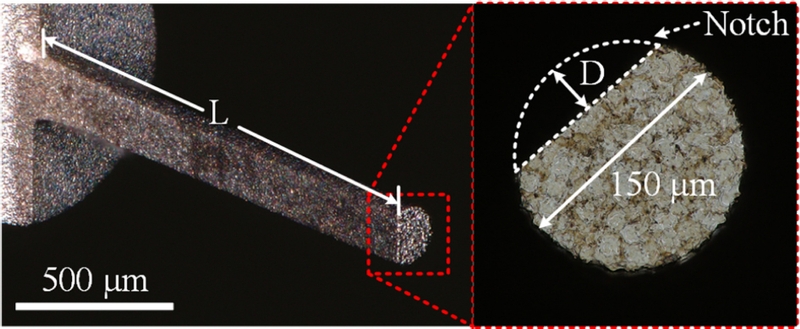
Debris flushing affects the geometric accuracy of the micro holes during EDM. Accordingly, a D-shaped electrode for enhancing debris flushing was fabricated through WEDG (Fig. 15). The Dshaped electrode with a notch with a height of 1,200 μm and a width of 35 μm was fabricated: If the notch height (L) is smaller than the depth of the machined micro holes, debris may rotate with the electrode instead of being flushed out of the hole. Conversely, if the notch width (D) is larger than the electrode’s radius, an unmachined area may form at the center of the micro hole.
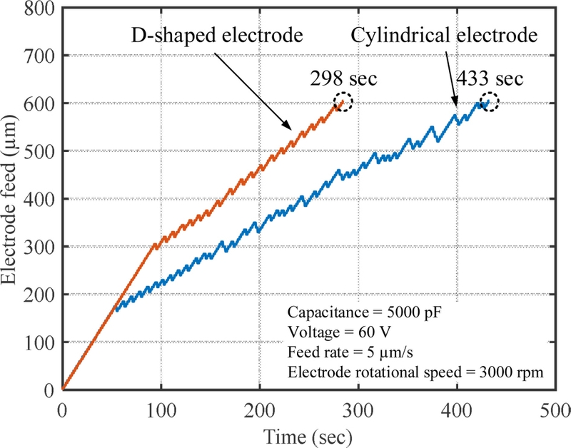
Fig. 16 shows the electrode feed position according to electrode shape. For both the cylindrical and D-shaped electrodes, a short circuit caused the electrode to rise after reaching a feed position of 175 and 305 μm, respectively. In the early stages of machining, the initial depth of the micro holes and the amount of generated debris were relatively small, allowing for superior debris flushing and preventing electrode rise due to short circuits. However, as machining progressed, the machined depth increased, and the amount of generated debris also increased. In this case, the Dshaped electrode enabled improved debris flushing and fewer short circuits compared to the cylindrical electrode, reducing machining time by 135 seconds. Furthermore, considering electrode wear length, the MRR of the cylindrical electrode and the D-shaped electrode was 29,300 and 35,993 μm3/s, respectively, with the Dshaped electrode achieving a higher MRR. Unlike the cylindrical electrode, the D-shaped electrode is more affected by electrical discharges concentrated at the electrode edge. However, the single notch facilitates smoother debris flushing. As a result, secondary discharges between the micro hole wall and the electrode are reduced. Since this influences the circularity of the machined micro hole, optimizing debris flushing by adjusting electrode geometry is crucial.
4.5 Application of EDM of Micro Holes
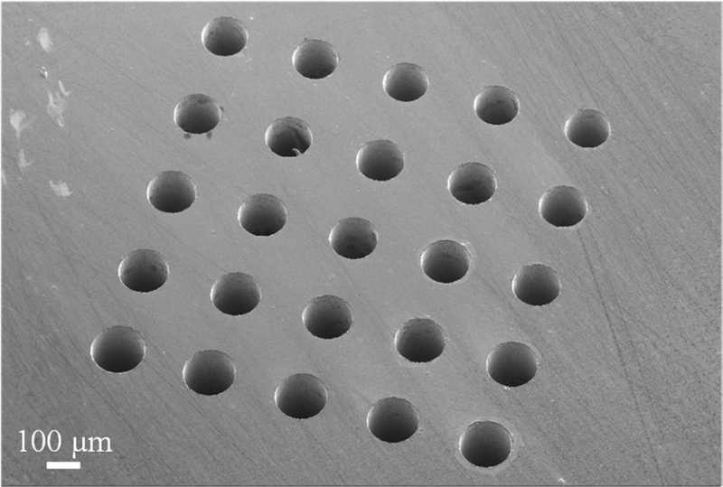
Fig. 17 shows the micro hole array machined using a D-shaped electrode. Micro holes with a diameter of 150 μm were machined at 300 μm intervals under the following machining conditions: applied voltage of 60 V, capacitance of 5,000 pF, electrode feed rate of 5 μm/s, and rotational speed of 3,000 rpm. The micro holes were machined to a depth of 600 μm with an average clearance of 4.578 μm. Enhanced debris flushing between the clearance and the notch of the D-shaped electrode minimized geometric errors at the micro hole entrance. The micro hole array can be used in the GMP process to manufacture micro pillars from glass materials with a constant gap and aspect ratio, eliminating the need for an antiadhesion coating [31].
5. Conclusions
This study investigated the EDM characteristics in EDM drilling of GC and a micro-hole array was successfully machined on GC. This study offers fundamental insights for optimizing EDM conditions in micro-hole fabrication on GC and contribute to the advancement of micro-fabrication techniques for GC-based micro components. From this research, the following conclusions can be drawn:
1. As the capacitance increased, the machining time decreased and the MRR increased due to the increased discharge energy. Additionally, EWR, clearance and surface roughness increased.
2. As the voltage increased, the machining time decreased and the MRR increased due to the increased discharge energy. However, the WER tended to increase as the voltage decreases, with the highest EWR observed under the applied voltage of 60 V. Furthermore, clearance didn’t change significantly.
3. Lower voltage or reduced discharge energy increases the occurrence of short circuits. These short circuits cause unstable machining, potentially degrading machining accuracy and surface quality. Additionally, frequent short circuits result in concaveshaped wear at the bottom center of the tool electrode, while the machined area develops a cone-shaped extrusion. Raman spectroscopy analysis confirmed the adhesion of tool electrode material on the extruded surface.
4. The D-shaped electrode reduced short circuits by improving debris flushing, thereby enhancing machining stability and precision in the EDM process for micro-hole fabrication on GC.
Acknowledgments
This work was supported by the National Research Foundation of Korea (NRF) grant funded by the Korea government (MSIT) (No. 2022R1F1A1067961).
REFERENCES
-
Dietrich, T., Ehrfeld, W., Lacher, M., Krämer, M., Speit, B., (1996), Fabrication technologies for microsystems utilizing photoetchable glass, Microelectronic Engineering, 30(1-4), 497-504.
[https://doi.org/10.1016/0167-9317(95)00295-2]

-
Li, J., Yang, K., Lian, G., Gong, F., Yang, G., (2023), A novel hot embossing process for producing high-quality glass micropillar arrays, Journal of Cleaner Production, 421, 138509.
[https://doi.org/10.1016/j.jclepro.2023.138509]

-
Lee, U. S., Sim, D. B., Lee, J. H., Kim, B. H., (2024), Fabrication of micro carbon mold for glass-based micro hole array, Micromachines, 15(2), 194.
[https://doi.org/10.3390/mi15020194]

-
Haq, M. R., Kim, Y. K., Kim, J., Ju, J. H., Kim, S. M., (2019), Fabrication of all glass microfluidic device with superior chemical and mechanical resistances by glass molding with vitreous carbon mold, Journal of Micromechanics and Microengineering, 29(7), 075010.
[https://doi.org/10.1088/1361-6439/ab1f99]

-
Beiring, P., Yan, J., (2019), Ultrasonic vibration-assisted microgrinding of glassy carbon, Proceedings of the Institution of Mechanical Engineers, Part C: Journal of Mechanical Engineering Science, 233(12), 4165-4175.
[https://doi.org/10.1177/0954406218823240]

-
Tseng, S.-F., Chen, M.-F., Hsiao, W.-T., Huang, C.-Y., Yang, C.- H., Chen, Y.-S., (2014), Laser micromilling of convex microfluidic channels onto glassy carbon for glass molding dies, Optics and Lasers in Engineering, 57, 58-63.
[https://doi.org/10.1016/j.optlaseng.2013.11.011]

-
Youn, S. W., Takahashi, M., Goto, H., Maeda, R., (2006), A study on focused ion beam milling of glassy carbon molds for the thermal imprinting of quartz and borosilicate glasses, Journal of Micromechanics and Microengineering, 16(12), 2576.
[https://doi.org/10.1088/0960-1317/16/12/009]

- Kim, S., Chung, D. K., Kim, B. H., Oh, K. H., Jeong, S., Chu, C. N., (2009), Micromachining using hybrid of laser beam and electrical discharge machining, Journal of the Korean Society for Precision Engineering, 26(10), 108-115.
- Doan, C. X., Kim, B. H., Chung, D. K., Chu, C. N., (2011), Fabrication of PCD micro tool and its hybrid micro machining, Journal of the Korean Society for Precision Engineering, 28(6), 694-700.
-
Park, J. W., Chung, D. K., Kim, B. H., Ok, J. G., Kim, W. J., Kim, Y. H., Chu, C. N., (2012), Wire electrical discharge machining of carbon nanofiber mats for field emission, International Journal of Precision Engineering and Manufacturing, 13(4), 593-599.
[https://doi.org/10.1007/s12541-012-0076-5]

-
Park, J. A., Lee, U. S., Kim, B. H., (2020), Micro pin fabrication of tungsten carbide using polycrystalline diamond, Journal of the Korean Society for Precision Engineering, 37(11), 791-796.
[https://doi.org/10.7736/JKSPE.020.085]

-
Na, Y., Kim, B. H., (2019), Effect of vibration and machining area in the fabrication of micro tool by reverse EDM, Journal of the Korean Society for Precision Engineering, 36(2), 169-175.
[https://doi.org/10.7736/KSPE.2019.36.2.169]

-
Lee, J. H., Yang, C. Y., Kim, B. H., (2024), Machining characteristics of micro EDM of silicon carbide, Journal of the Korean Society for Precision Engineering, 41(2), 131-137.
[https://doi.org/10.7736/JKSPE.023.137]

-
Muramatsu, S., Ito, H., Sugimoto, K.-I., Osaka, H., Sato, T., (2010), Electrical discharge machining of glass-like carbon die, Journal of the Japan Society for Precision Engineering, 76(1), 96-100.
[https://doi.org/10.2493/jjspe.76.96]

-
Lee, U. S., Yang, C. Y., Lee, J. H., Kim, B. H., (2021), Micro drilling of single crystal SiC using polycrystalline diamond tool, Journal of the Korean Society for Precision Engineering, 38(7), 471-478.
[https://doi.org/10.7736/JKSPE.021.013]

-
Schueller, O. J., Brittain, S. T., Whitesides, G. M., (1999), Fabrication of glassy carbon microstructures by soft lithography, Sensors and Actuators A: Physical, 72(2), 125-139.
[https://doi.org/10.1016/S0924-4247(98)00218-0]

-
Kim, M. K., Yang, C. Y., Sim, D. B., Lee, J. H., Kim, B. H., (2024), Study on micro grooving of tungsten carbide using disk tool, Journal of the Korean Society for Precision Engineering, 41(2), 123-129.
[https://doi.org/10.7736/JKSPE.023.138]

-
Dae Bo, S., Chan Young, Y., Bo Hyun, K., (2022), Machining of V-shaped microchannel on cemented carbide using PCD tools, Journal of the Korean Society for Precision Engineering, 39(10), 747-752.
[https://doi.org/10.7736/JKSPE.022.083]

-
Kumar, K., Batra, U., (2019), Fabrication of high aspect ratio WC-Co micro electrodes for μ-EDM application, Materials Today: Proceedings, 18, 2970-2976.
[https://doi.org/10.1016/j.matpr.2019.07.167]

-
Li, G., Natsu, W., Yang, J., Yu, Z., (2022), Bubble flushing effect in micro EDM drilling and its relation with debris, Journal of Materials Processing Technology, 305, 117590.
[https://doi.org/10.1016/j.jmatprotec.2022.117590]

- Kim, G. M., Kim, B. H., Chu, C. N., (1999), Machining rate and electrode wear characteristics in micro-EDM of micro holes, Journal of the Korean Society for Precision Engineering, 6(10), 94-100.
-
Murray, J., Zdebski, D., Clare, A., (2012), Workpiece debris deposition on tool electrodes and secondary discharge phenomena in micro-EDM, Journal of Materials Processing Technology, 212(7), 1537-1547.
[https://doi.org/10.1016/j.jmatprotec.2012.02.019]

-
Liu, H., Bai, J., (2020), The tool electrode wear and gap fluid field simulation analysis in micro-EDM drilling of micro-hole array, Procedia CIRP, 95, 220-225.
[https://doi.org/10.1016/j.procir.2020.02.278]

-
Wang, K., Zhang, Q., Zhu, G., Huang, Y., Zhang, J., (2018), Influence of tool size on machining characteristics of micro- EDM, Procedia CIRP, 68, 604-609.
[https://doi.org/10.1016/j.procir.2017.12.122]

-
Hou, S., Bai, J., (2020), Experimental investigation on electrode wear of array holes machining in micro-EDM, Procedia CIRP, 95, 527-532.
[https://doi.org/10.1016/j.procir.2020.02.297]

-
Zou, Z., Zhang, X., Chan, K., Yue, T., Guo, Z., Weng, C., Liu, J., (2023), An analysis of the uneven tool electrode wear mechanism in the micro-electrical discharge machining process, International Journal of Precision Engineering and Manufacturing- Green Technology, 10(6), 1375-1391.
[https://doi.org/10.1007/s40684-022-00499-9]

- Lim, J. H., Ryu, S. H., Je, S. U., Chu, C. N., (2003), Distortion of the bottom surface in micro cavity machining using MEDM, Journal of the Korean Society for Precision Engineering, 20(12), 191-197.
-
Liew, P. J., Yan, J., Kuriyagawa, T., (2013), Carbon nanofiber assisted micro electro discharge machining of reaction-bonded silicon carbide, Journal of Materials Processing Technology, 213(7), 1076-1087.
[https://doi.org/10.1016/j.jmatprotec.2013.02.004]

-
Wang, Y., Xi, X., Zhang, L., Nie, Z., (2024), Preparation of tungsten carbide powder by In situ electrolysis utilizing selfconsuming graphite anode, Metallurgical and Materials Transactions B, 1-11.
[https://doi.org/10.1007/s11663-024-03040-2]

-
Baserga, A., Russo, V., Di Fonzo, F., Bailini, A., Cattaneo, D., Casari, C. S., Bassi, A. L., Bottani, C. E., (2007), Nanostructured tungsten oxide with controlled properties: Synthesis and Raman characterization, Thin Solid Films, 515(16), 6465-6469.
[https://doi.org/10.1016/j.tsf.2006.11.067]

-
Asgar, M. A., Kim, Y. K., Jin, C., Kim, J., Byeon, S., Ali, M., Hussain, T., Kim, S.-M., (2022), Fabrication of vitreous carbon mold for glass moled microarray, 2022 13th International Conference on Information and Communication Technology Convergence (ICTC), 1151-1153.
[https://doi.org/10.1109/ICTC55196.2022.9952495]


M.S. student in the Department of Mechanical Engineering, Graduate School, Soongsil University, Korea. His research interest in micro machining.
E-mail: Kimjyprema@soongsil.ac.kr

M.S. student in the Department of Mechanical Engineering, Graduate School, Soongsil University, Korea. Her research interest is micro machining.
E-mail: jihyolee@soongsil.ac.kr

Professor in the School of Mechanical Engineering, Soongsil University, Korea. His research interests include micro mechanical machining processes and advanced manufacturing processes, including micro electrical discharge machining (EDM), electrochemical machining (ECM), and electrochemical discharge machining (ECDM).
E-mail: bhkim@ssu.ac.kr

