A Study on Photocurable Liquid-Crystal-on-Silicon (LCoS) Microdisplay Based Stereolithography Type 3D Printer for Fabrication of Microfluidic Channel Systems
Copyright © The Korean Society for Precision Engineering
This is an Open-Access article distributed under the terms of the Creative Commons Attribution Non-Commercial License (http://creativecommons.org/licenses/by-nc/3.0) which permits unrestricted non-commercial use, distribution, and reproduction in any medium, provided the original work is properly cited.
Abstract
A microfluidics chip is a miniature analytical system that injects a small amount of reagent into microchannels formed in the chip. It controls fluid flow to perform pretreatment, detection, reaction, mixing, separation, and analysis in parallel. In this study, polygonal microchannel structures were fabricated using a microstereolithography 3D printer based on an LCoS microdisplay projector. In the experiment, the width of the microchannel structure was changed from 50 μm to 500 μm, and the output and width of the structure were measured. Inspection of the shape of the resulting microchannel structure showed that the tip of the structure was elliptical instead of the expected rectangular shape, and the fabrication width error increased as the channel width decreased to 200 μm or less. Nevertheless, it was possible to fabricate microfluidics chip structures with widths less than 100 μm. The results of this study demonstrate the applicability of an LCoS microdisplay project-based 3D printer for the fabrication of microfluidic channel structures.
Keywords:
LCoS, Microdisplay, 3D printer, Microfluidics, Biochip, Stereolithography1. Introduction
The work and living environment of the entire world’s population is undergoing significant changes due to 2020 Covid-19 pandemic. Owing to its high contagiousness at the onset of the infection compared to SARS and MERS outbreaks, newly confirmed cases of COVID-19 is still spreading at a rate of hundreds in Korea and hundreds of thousands daily around the world. Diagnostic methods for determining COVID-19 infection can be largely divided into either RTPCR (Real Time-Polymerase Chain Reaction) test or self-diagnostic test using immunochromatography. The PCR test takes 6 to 12 hours, and the self-diagnostic test can produce results in a significantly shorter amount of time at the cost of lower accuracy. Thus, DNA biosensor technology is being developed to compensate for this disadvantage. As with DNA biosensor technology, research and development of micro-total analysis systems (μTAS), bio-imaging, and biochips are required to rapidly develop diagnostic, vaccine, and therapeutic technologies in the event of another future pandemic [1,2]. A microfluidics chip is a type of biochip that constitutes a small-scale analysis system that can produce real-time analytical results by enabling the pretreatment, detection, reaction, mixing, and separation of liquid sample by injecting a small amount of reagent into a microchannel formed on the chip surface to control the flow of fluid [3]. Microfluidics chip is fabricated by techniques such as deposition, photolithography, soft-lithography, etching, and nano-imprinting generally used in semiconductor manufacturing processes. A microchannel is formed on silicon wafer, glass, or polydimethylsiloxane (PDMS). The fabrication process takes 2-3 days, which is disadvantageous for mass production. Moreover, there is another disadvantage of high manufacturing cost due to the requirement of a semiconductor fabrication quality clean room facility and equipment [4]. Micro-stereolithographic 3D printer projects a two-dimensional image made up of micrometersized pixels on the bottom of a clear tank containing a photocurable resin, and the resin layer plane that is exposed to the projected light hardens with exposure to two-dimensional images to form stacked three-dimensional structure. Microfluidics chip manufacturing using this technology is advantageous for cost reduction and mass productivition compared to existing manufacturing methods and can increase the degree of freedom in the shape of the realizable structure [5]. The semiconductor device density and pixel size of the microdisplay greatly affect the precision of the 3D printed structure because the pixels are enlarged when the twodimensional image created from the screen display device is projected through the projection lens. In the past, LCD (Liquid-Crystal Display) and DMD (Digital Micromirror Device) were mainly used as screen display devices. The light-transmitting LCD is not suitable for structures that require precision due to its large pixel size and low contrast ratio. Although the lightreflecting DMD has a small pixel size and high contrast ratio, the structure is complicated because tiltable micro-mirror structures are integrated on the device surface to reflect light. In addition, since static random access memory (SRAM) composed of 6 transistors (TRs) is used to drive the pixels of the DMD, it is not easy to configure TRs in micrometer-sized pixels and the driving voltage is 5-20 V, limiting the pixel miniaturization. The miniaturization of the TR and micro-mirror can increase the resolution of the screen display device by reducing the size of the pixel. In addition, since resolution is intimately related to the precision of 3D printed structures, the inadequate scalability to ultra-high resolution of DMD technology imposes limitations for production of microfluidics chips which need to be able to handle microscale and nanoscale fluid motions [6,7]. In this study, a micro-stereolithographic 3D printer was constructed using an LCoS (Liquid-Crystal-on-Silicon) microdisplay with a resolution of 1,920 × 1,080 pixels as the projector's screen display device. LCoS consists of TR and addressing logic circuitry on a silicon wafer, so it is possible to realize very small pixels due to its high degree of integration. With this advantage, LCoS can implement pixels that are much smaller than LCD and relatively smaller than DMD. In addition, since the TR can be miniaturized with a driving voltage of 5 V or less, it is better suited for implementation of ultra-high resolution display architecture. Therefore, we studied the performance of a micro-stereolithographic 3D printer that can form microchannels, the primary feature of microfluidics chips, by constructing an LCoS-based projection system.
2. Experimental Method
2.1 Fabrication of LCoS Microdisplay
The semiconductor process is largely divided into a frontend process of forming an integrated circuit on a silicon wafer and a backend process of packaging the silicon wafer into the form of a chip. In this study, a silicon wafer was supplied from a foundry that performs the frontend process and LCoS microdisplay was packaged through the backend process. In order to perform the backend process to form the LCoS, a semiconductor-class clean room facility is required. The structure and role of the facility are as follows:
1) FFU (Fan Filter Unit) System: A small fan and HEPA (High Efficiency Particulate Air) filter or ULPA (Ultra-Low Penetration Air) filter are combined and are usually installed on the ceiling. The system removes airborne dust (Particulates) and microorganisms and maintains the room air at positive pressure;
2) Thermo-hygrostat: A system that controls the temperature and humidity inside the working environment and ventilates the enclosed environment;
3) Air shower: A cleaning facility used by workers before entering the clean room to remove dust and foreign substances.
The class of the cleanroom facility is shown in Table 1, and the semiconductor packaging steps are divided according to the class. By federal standards, cleanroom classification is set according to the number of dust particulates larger than 0.5 μm contained within 1 cu. Ft. of volume space.
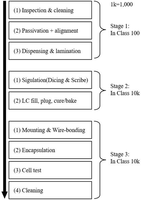
The backend packaging process of LCoS microdisplay is outlined in Figure 1. The backend process is divided into three major stages. The details of each stage are as follows:
1) Stage 1:
(1) Clean the inside of the electron-beam coating chamber with a vacuum cleaner, a scrubber, or isopropyl alcohol (IPA). Then, clean the indium tin oxide (ITO) film coated glass surface of the same size as the 8-inch silicon wafer with a filtered air gun and then clean with IPA;
(2) The cleaned silicon wafer and ITO glass are placed at a certain angle, and the silicon dioxide (SiO2) passivation layer is coated with an electron beam in a high vacuum (about 2 × 10⁻⁶ Torr) state, and then the deposition rate is increased to form an anchoring layer to secure the liquid crystal;
(3) Mix the optical bond (NOA 81, NORLAND, USA) with the 2.5 μm spacer, avoiding spacer agglomeration, and then fill the mixed optical bond into the inner syringe of the dispenser. Place the ITO glass on the stage of the dispenser and apply the optical bond seal line to the ITO glass with the set program along the perimeter of the display surface. Place the silicon wafer on the lamination station and align and fix the ITO glass on it. Figure 2 shows the processes described above.

Illustration of the process step involving the alignment and lamination of ITO glass onto a CMOS backplane chip
2) Stage 2:
(1) Place the laminated ITO-silicon wafer on the inner stage of the dicing saw and make partial notch cuts along the scribe lanes on the backside of the silicon wafer. After transferring the silicon wafer to the Scribe Station equipment, scribe additional break lines along the lane with a tungsten scribe wheel, and then use a rubber-coated breaker tongs to separate the laminated silicon wafer into singulated chips;
(2) Fill the singulated chips with liquid crystal through the open part of the seal line into the empty space between the silicon wafer and the ITO glass, and plug the opening with the optical bond.
3) Stage 3:
(1) Mix room temperature curable silicone with 15 μm spacer, place it in a syringe, and apply it to the prepared PCB (Printed Circuit Board). Place a completed chip on the PCB, press it with a vacuum press for about 1 minute, and then cure it at room temperature for 1 hour. Then, using a wire bonder, connect the electrode between the unit chip and the PCB;
(2) Apply an optical bond on the exposed lead wire and cure for 10 seconds, then apply a second coat of room temperature curable silicone and cure at room temperature for 3 hours;
(3) Connect the completed LCoS microdisplay and the Control Board with an MCX (Micro Coaxial) cable, and input a test image to the Control Board to check whether the test image is displayed on the LCoS microdisplay and check for defective pixels;
(4) The normal product that has passed the above test is cleaned and packaged.
2.2 LCoS projector operating principle
Figure 3 illustrates the structure of an LCoS microdisplay. LCoS is a reflection-type screen display device in which liquid crystal is applied between a glass coated with electrically conductive indium tin oxide (ITO) and a silicon wafer. The operation of a pixel in the display is as follows:
1) A 2D image signal is inserted into the Control Board that controls the LCoS microdisplay;
2) Voltage is applied to the integrated circuit of each pixel according to the pixel information of the input image;
3) When TR is on, an electric field is generated between the ITO glass and the silicon wafer to adjust the angle of the liquid crystal. The phase of the normally incident polarized light is modulated through reflection as the refractive index experienced by the incident light varies according to the angle of the liquid crystal.
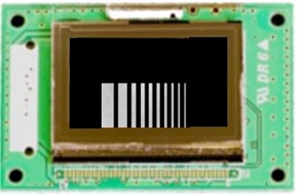
For example, when a two-dimensional image signal representing 10 rectangles of different widths is input to LCoS, the pixels with TR in ‘on’ state will display rectangles as shown in Figure 4 on the surface.
The operational principle of the LCoS projector is as follows:
1) Since liquid crystal does not emit light on its own, an external illumination source is needed to project an image;
2) When the light from the illumination source passes through the imaging lens and hits the PBS (Polarizing Beam Splitter), the reflected polarized light is directed to the LCoS microdisplay;
3) Pixels in ‘on’ state modulate the phase of the incident polarized light as it is reflected from the top aluminum layer of the silicon backplane through the liquid crystal, changing the angle of the polarization by 90 degrees, to pass through PBS and expand according to the magnification of the projection lens to form a 2-dimensional image on the projection plane.
2.3 Micro Stereolithographic 3D Printer Prototype System
Fig. 5(a) shows the micro stereolithography 3D printer prototype system, and Fig. 5(b) shows the exposure module that implements an LCoS microdisplay. The shown stereolithography 3D printer consists of an LCoS projector, a build plate that can move up and down, and a vat containing ultraviolet (UV) light-curing resin. In order to produce a solid model using 3D printer, a 3D model of the solid is first drawn using a CAD program and saved as a data file. The saved file is then loaded into a Slicer program and sliced to form a 3-dimensional model consisting of multiple layers of 2-dimensional image in preset thickness increment.
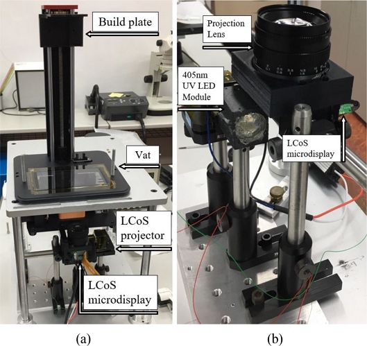
Photographs of (a) the LCoS 3D printer prototype and (b) LCoS microdisplay-based exposure module used in this study
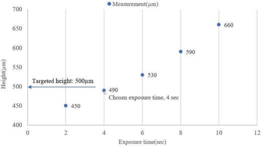
Prior to microchannel printing, stereolithography 3D printers may have deposits in the vat surface or structural overgrowths depending on the exposure (Curing) time. In order to determine the optimal curing time to prevent these phenomena, the exposure time experiment outlined in Table 2 was performed. The first 4 of a total of 10 layers are cured to form a secure adhesion layer on the build plate--the exposure time for the adhesion layers was set to 8 seconds based on prior experimentation.
In order to stack the cross-sectional images of the microchannel, the build plate of the vat containing photo-curable resin is lowered to a single layer height (50 μm) from the bottom of the vat and exposed with the image projected by the LCoS exposure module. Subsequently, the build plate is incrementally raised by the layer thickness, and the structure is created by repeating the operation of exposing and curing the cross-sectional image of corresponding layers to form a 3-dimensional solid [8].
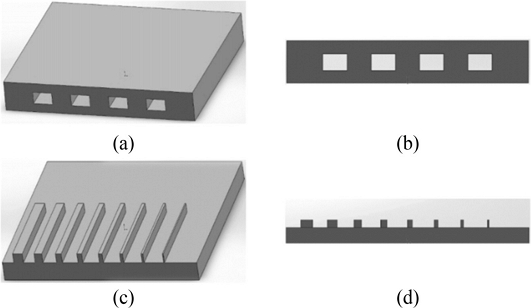
Figures 6(a) and 6(b) illustrates 3D diagrams of an ideal microchannel structure. In the experiment of this study, structures shown in Figures 6(c) and 6(d), although not suitable as microchannels, which allow the observation of the dimension and rigidity of the building blocks of the photocurable resin solution were formed. As embodied in Fig. 6(c), on a rectangular base having a size of 10 × 10 × 1 mm (Width × Length × Height), rectangular strips of 5 mm length, 0.5 mm height, and widths of 500, 400, 300, 250, 200, 150, 100, 50 [μm] were drawn and printed using the configured equipment, and the widths of the resulting structure were measured.
3. Result and discussion
In this study, the optimal exposure time of 4 seconds which resulted in the smallest deviation from the target value as shown by Figure 7 was utilized. Excluding the base layer curing time and the translation time of the build plate, a 3-dimensional model can be fabricated at a rate of 12.5 μm/sec. (Volumetric Height) with the optimal exposure time.
The LCoS microdisplay-based exposure module of the prototype micro-stereolithographic 3D printer consists of a 405 nm wavelength UV LED as the light source and an off-the-shelf F/1.4 camera lens with a 50 mm focal length for image projection. About 22% of the UV LED's maximum output of 5 W is passed by the F/1.4 optical system, and taking into account the LCoS reflectance and polarization loss of about 70%, the LCoS projector will deliver about 6.5% or about 320 mW of the light emitted by the LED onto the 3D printing area.
The measured optical power density at the bottom of the tank was 0.08 mW/mm2 for a projected image of 50 × 70 mm, which corresponds to a total output of about 280 mW and is within 13% of the expected value of 320 mW. The contrast ratio was about 300 : 1, and by re-adjusting the throw distance and refocusing the projection lens, the diagonal size of the projected image can be adjusted from 0.87" (22.1 mm) to 7" (177.8 mm).
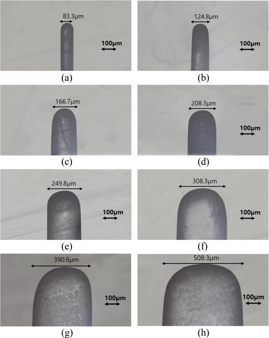
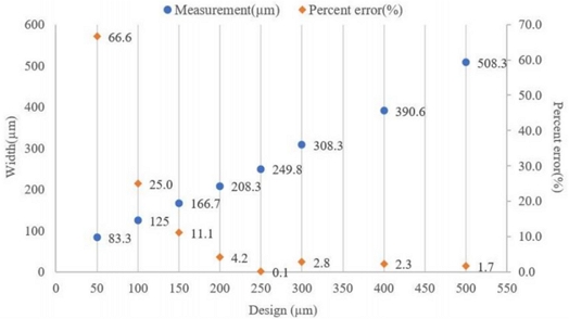
As shown in Figure 8, the cross-section of the resulting microchannel formed an elliptical shape, and the parametric chart in Figure 9 compares the measured widths to the design widths of the microchannel and plots the percent error.
The percent area in the Figure 9 was calculated by following the equation:
| (1) |
The reason that the error increases for feature widths less than 200 μm is likely due the greater the influence of obliquely incident light (about ±21 degrees) of F/1.4 illumination to the area outside of the edge of the feature. That is, ±21 degree oblique incidence light passing through the layer thickness of 51 μm spreads the width of the microchannel implemented on the screen by as much as 19 μm on each side, and likely had an effect of curing up to a total of 38 μm of width outside of the feature. Thus, as the width of the shape to be printed becomes narrower, a significant amount of light that should be projected into the shape leaks out beyond the edge of the shape, and the photopolymer in the region outside the shape is partially hardened. In particular, the results for less than 250 μm wide shapes in Figure 9, clearly follows a linear trend. By applying the linear curve fit to this data, we can establish the relationship w' = 0.8326 w+41.73 (w' = output width; w = design width). In order to reduce the error rate, it will be necessary to reduce the layer thickness, implement a higher F/# optics, and control the exposure time in decimal units. In particular, the dimensional error for 50 μm and 100 μm structures is more than 25%, but nevertheless, this result represents an important achievement by demonstrating the fabrication of structures with less than 100 μm features by Micro-stereolithographic 3D printer with LCoS exposure module for microchannel formation. According to the performance results of the FHD (1,920 × 1,080) resolution LCoS microdisplay used in this study, further research is needed to investigate the applicability of UHD (4,096 × 2,160) resolution LCoS microdisplay for development of more precise 3D printing technology for microfluidics chip fabrication.
4. Conclusion
While the direct use of MFC devices fabricated using conventional photocurable resin may be limited due to its vulnerability to some solvents and reagents, ongoing efforts to expand the range of available materials from nylons to ceramic suspensions and associated post-processing is expected to expand its applicability. Also, 3D printed resin structure can be duplicated into base materials such as glass and silicon substrate using reactive ion etching (RIE), using combinations of gases such as CHF3 (for glass), SF6 (for silicon), and O2 (for resin) in appropriate proportions to control the relative etch rates, or by direct ion beam etching (IBE) or chemically-assisted ion beam etching (CAIBE), It may also be possible to replicate the 3D printed structure directly into PDMS by a method similar to that using complimentary shapes etched into glass [9].
In this study, a two-dimensional image generator was fabricated using an LCoS microdisplay and a method to fabricate micro-channel was studied by prototyping a micro-stereolithographic 3D printer. As a result of the study, it was observed that cured resin deposits were formed in the vat and overgrowths resulted depending on the curing time, and the test structures of narrow microchannel were observed to collapse easily even when the exposure time was optimized. In order to resolve these issues, it is necessary to carry out further research to improve the precision of the studied fabrication method by implementing a higher resolution LCoS microdisplay, control the viscosity of the UV resin, control the vertical movement of the build plate, and improve the curing method.
Micro-stereolithographic 3D printer using LCoS projection module is promising for mass production of microfluidic channel devices as it can harden complex shapes in units of planar surfaces with single exposure for each layer. In the future, we plan to use a UHD resolution LCoS microdisplay that has 4 times actual number of pixels than the available DMD component to increase the precision to control the formation of microchannels more precisely.
REFERENCES
- Biotech Policy Research Center, (2021), Bio-future promising technology (Report No. 2021-55). https://www.bioin.or.kr/index.do
- Biotech Policy Research Center, (2009), Bio-nano Convergence Technology (Report No. 2008-5). https://www.bioin.or.kr/index.do
- Lee, E. Y., (2010), Principle and application of microfluidics-based cell chip, News & Information for Chemical Engineers, 28(6), 678-684. https://www.cheric.org/PDF/NICE/NI28/NI28-6-0678.pdf
- Laser Application Center, Trend report in Microfluidics. https://lac.or.kr/page/board/board.php?bo_id=lac_tech&wr_id=2405
-
Park, J., Park, H., (2017), Liquid flow characteristics in 3D-printed rectangular microchannel, Transactions of the Korean Society of Mechanical Engineers B, 41(1), 69-74.
[https://doi.org/10.3795/KSME-B.2017.41.1.069]

- Joo, J., Kim, S., Jeong, S., (2006), Digital micromirror device based microstereolithography for the fabrication of 3D microstructures, Laser Solutions, 9(1), 1-7.
- Hwang, C., Kim, Y., Kim, G., Yang, J., Pi, J., Hwang, C., Choi, J., Kim, J., (2016), Large area spatial light modulator panel for digital holography, Electronics and Telecommunications Trends, 31(6), 48-56.
-
Shin, D.-H., Park, Y.-M., Park, S.-H., (2018), Correlation between UV-dose and shrinkage amounts of post-curing process for precise fabrication of dental model using DLP 3D printer, Journal of the Korean Society of Manufacturing Process Engineers, 17(2), 47-53.
[https://doi.org/10.14775/ksmpe.2018.17.2.047]

-
Oyama, T. G., Hinata, T., Nagasawa, N., Oshima, A., Washio, M., Tagawa, S., Taguchi, M., (2013), Micro/nanofabrication of poly (L-lactic acid) using focused ion beam direct etching, Applied Physics Letters, 103(16), 163105.
[https://doi.org/10.1063/1.4825277]


Ph.D candidate in the Department of Environmental Protection, Gyeongsang National University. His research interest is 3D printer.
E-mail: khw910813@gnu.ac.kr

Professor in the Department of Environmental Protection, Gyeongsang National University.
E-mail: d-klee@gnu.ac.kr


